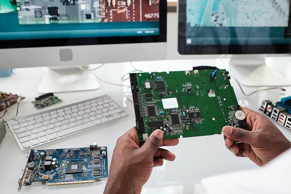
 Design for Manufacturing (DFM) in PCB design refers to the practice of creating printed circuit boards that can be manufactured, assembled, and tested efficiently and reliably, without unnecessary cost or risk. While a circuit may function perfectly on paper, poor manufacturability can quickly turn a promising design into a costly problem once it reaches production.
In today’s fast-moving electronics industry, PCB DFM is critical. It directly impacts manufacturing cost, product reliability, production yield, and lead times. Designs that fail to consider manufacturing constraints often result in PCB manufacturing issues such as low yields, assembly errors, or unexpected delays all of which can significantly affect project schedules and budgets.
A common misconception is that design for manufacturing PCB considerations are solely the responsibility of the PCB manufacturer. In reality, effective DFM is a shared responsibility between the PCB designer and the manufacturing partner.
When DFM is overlooked during the design stage, the consequences are real and immediate: design re-spins, increased costs, extended lead times, and avoidable frustration. Integrating DFM from the outset is key to delivering boards that work not just electrically, but commercially too.
What Is Design for Manufacturing (DFM) in PCB Design?
Design for Manufacturing (DFM) in PCB design is the discipline of ensuring that a printed circuit board can be manufactured consistently, cost-effectively, and at scale, without compromising performance or reliability. It goes beyond simply meeting electrical requirements and focuses on aligning the design with real-world fabrication and assembly capabilities.
Within the wider PCB design process, DFM sits alongside two closely related disciplines. DFM (Design for Manufacturing) addresses how the bare PCB is fabricated, including materials, stack-up, drill sizes, and design rules. DFA (Design for Assembly) focuses on how components are placed, soldered, and assembled efficiently.
DFT (Design for Test) ensures the finished board can be tested reliably, both during production and in the field. Together, these approaches help reduce risk across the entire product lifecycle.
Crucially, DFM should not be treated as a final check before files are sent to manufacture. It is most effective when applied early in the PCB design process, influencing decisions from schematic capture through layout and component selection.
Early adherence to proven PCB DFM guidelines allows design teams to avoid costly redesigns, streamline production, and move smoothly from prototype to volume manufacture, especially when design and manufacturing expertise are closely aligned from the outset.
The Cost of Ignoring DFM: Real-World Consequences
When Design for Manufacturing is overlooked, the impact is rarely theoretical, it shows up quickly and often expensively. From a manufacturing perspective, these issues are seen time and time again once a design reaches the factory floor.
One of the most common PCB manufacturing problems is unexpected cost increases. Designs that push tolerances, use hard-to-source components, or require special processes often cost far more to build than anticipated. What looked economical during design can become expensive in production.
Ignoring DFM also leads to longer lead times. Manufacturers may need to pause production to clarify design issues, request changes, or wait for alternative components. In many cases, this results in PCB re-spins, where the board must be redesigned and re-manufactured. PCB re-spin costs quickly add up, not only in money but in lost time and missed market opportunities.
There are also risks to quality and reliability. Poor yields, inconsistent assembly, and early-life failures are common outcomes of designs that are not manufacturing-friendly. Ultimately, these issues affect customer confidence and brand reputation.
This is why manufacturers consistently emphasise one principle: first-time-right matters. Designs that consider DFM from the start move through production smoothly, reduce risk, and deliver predictable, reliable results.
Key DFM Considerations Every PCB Engineer Should Know
Design for Manufacturing is not a single check at the end of a project. It is a collection of practical decisions made throughout the design process that directly affect how smoothly a board can be built. Below are some of the most important DFM considerations that consistently influence manufacturing success.
Component Selection & Availability
Effective PCB component selection is one of the earliest and most important DFM decisions. While many components may appear electrically suitable, not all are practical for manufacturing. Certain package types are preferred because they are easier to place, solder, and inspect in volume production.
Using obsolete or hard-to-source components introduces unnecessary risk. Even if a part is available during prototyping, it may cause delays or redesigns when moving to production. Manufacturers also consider component tolerances and always recommend following datasheet guidelines for land patterns and spacing.
This is why BOM optimisation is a core part of DFM. Reviewing the bill of materials early helps identify supply risks, cost drivers, and assembly challenges before they become production issues.
PCB Stack-Up & Materials
PCB stack-up design plays a major role in manufacturability. Standard stack-ups are widely supported by manufacturers and typically offer the best balance of cost, performance, and lead time. Custom stack-ups, while sometimes necessary, often increase complexity and cost.
Material choices also matter. Some PCB materials have longer lead times or limited availability, which can affect production schedules. For designs requiring controlled impedance, early coordination with the manufacturer ensures the stack-up can meet electrical requirements without unnecessary over-engineering.
Choosing suitable PCB materials with manufacturing in mind helps avoid delays and keeps costs predictable.
Track Widths, Spacing & Design Rules
Many PCB manufacturing issues arise when designs push track widths and spacing to theoretical minimums. While a design may pass design rule checks on screen, it may be difficult to manufacture consistently at scale.
Every manufacturer has defined capabilities and preferred limits. Designing within these limits improves yield and reliability. Early alignment of PCB design rules and PCB trace width spacing with the chosen fabricator helps prevent last-minute changes and unexpected problems during production.
In DFM, conservative, well-understood limits often lead to better results than pushing the edge of what is technically possible.
Via Types & Hole Sizes
Via selection has a direct impact on cost and manufacturability. Standard through-hole vias are the simplest and most economical option. Blind, buried, and microvias enable higher density designs but significantly increase fabrication complexity and cost.
Aspect ratio limits must also be respected to ensure reliable plating and drilling. In some cases, advanced via structures are justified, particularly for compact or high-speed designs. In others, they introduce unnecessary risk.
Good DFM practice is knowing when complexity is justified, and when it isn’t.
Solder Mask & Silkscreen Considerations
Solder mask and silkscreen may seem like minor details, but they have a significant impact on PCB assembly quality. Poor solder mask design is a common cause of solder bridging, short circuits, and rework during manufacturing.
Solder mask openings must be correctly sized to expose pads without encroaching on nearby features. If clearances are too tight, mask registration can become inconsistent, particularly on fine-pitch components, leading to unreliable solder joints. Following manufacturer recommendations for solder mask expansion helps improve yield and repeatability.
Silkscreen is used for component identification and inspection, but it must be applied carefully. Silkscreen printed over pads or too close to solder joints can interfere with soldering. Clear, readable markings that remain visible after assembly are ideal, but excessive detail can reduce manufacturability.
Good DFM strikes a balance between clarity and production practicality.
Panelisation & Board Outline
Panelisation is a key DFM consideration that directly affects assembly efficiency. While designers focus on individual PCBs, manufacturers build and assemble boards in panels to suit automated processes. Designs that ignore panelisation often require changes before production can begin.
A practical consideration for the PCB designer is keeping copper and components clear of the board edge. Panel rails, which sit outside the individual boards, are defined at the panelisation stage, but the board outline itself must accommodate the clearances required for handling and assembly. Designing with appropriate edge clearances avoids interference with assembly processes and reduces the risk of damage to edge-mounted features during panel separation.
Break-away tabs, mouse bites, or V-grooves must also be designed to allow clean separation without damaging the finished boards.
Designing with the manufacturer’s requirements in mind leads to smoother assembly, reduced handling issues, and more reliable production, all essential outcomes of effective Design for Manufacturing.
DFM for PCB Assembly (DFA): Designing for Smooth Assembly
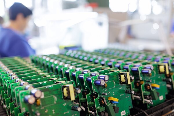
Design for Assembly (DFA) focuses on ensuring a PCB can be assembled efficiently, accurately, and repeatably in a production environment. While closely linked to DFM, PCB DFA specifically addresses how components are placed and soldered, and it plays a crucial role in achieving consistent quality at scale.
Component orientation is worth considering during layout, particularly for through-hole designs intended for wave soldering, where consistent orientation can simplify the process and reduce the risk of defects. For SMT designs, modern pick-and-place machines handle component orientation automatically during placement, though consistent orientation in the design can still reduce programming time during initial machine setup.
Pick-and-place optimisation also depends on sensible component spacing. Adequate clearance around connectors, large capacitors, and tall components allows placement nozzles and soldering equipment to operate without interference. Crowded layouts may work electrically, but they often create challenges during assembly and rework.
Soldering method selection is another key DFA consideration. Reflow soldering is ideal for most surface-mount designs, while wave soldering is typically used for through-hole components. Designs that mix technologies without planning can increase complexity and cost.
Finally, designs that rely heavily on hand-soldering introduce risk in production volumes. Manual processes are slower, less repeatable, and more prone to defects. Effective PCB DFA minimises manual intervention, resulting in faster assembly, higher yields, and more reliable products.
DFM Checks Before Sending Files to Manufacture
Before a PCB design is released to production, a final review is essential to catch issues that may have been missed earlier. This stage can be thought of as the final DFM sanity check, a practical step that helps prevent avoidable delays, questions from the manufacturer, and costly rework.
Even well-designed boards can encounter problems if manufacturing files are incomplete or inconsistent. Taking the time to carry out a structured PCB DFM checklist ensures the design is truly ready for fabrication and assembly.
Key checks to complete before release include:
- Design Rule Check (DRC) passed, aligned with the manufacturer’s capabilities
- Stack-up confirmed, including materials, thickness, and impedance requirements
- Drill files verified, with correct hole sizes and tolerances
- Gerbers reviewed visually to confirm layers, polarity, and alignment
- Assembly drawings complete, clearly showing component placement and orientation
- Pick-and-place files correct, with accurate coordinates and rotations
A careful PCB Gerber review at this stage often highlights issues that automated checks cannot. Performing these final DFM checks helps ensure a smooth handover to manufacturing, reduces back-and-forth communication, and increases the likelihood of first-time-right production.
Designing PCBs That Are Ready for the Real World
Design for Manufacturing is not just a technical exercise, it is a practical mindset that ensures PCBs are ready to perform in the real world. By considering manufacturability from the earliest design stages, engineers can avoid unnecessary delays, control costs, and achieve the first-time-right outcomes that modern product development demands. Proactive DFM thinking reduces risk, improves reliability, and allows designs to move smoothly from concept to production.
Working with a PCB design partner who understands manufacturing realities adds further value. Experience across multiple manufacturers enables informed decisions that balance performance, cost, and lead time.
Early engagement also helps identify potential issues before they become expensive redesigns, acting as a vital bridge between design intent and production capability.
At DSL Electronic Design, DFM is embedded throughout our professional PCB design process. By aligning design and manufacturing from the outset, we help clients reduce time to market, minimise risk, and deliver production-ready designs.
To discuss manufacturability early and get more from your PCB design services in the UK, get in touch with our team.


